
WBG Semiconductors: Key Technology for High-Density and Eco-Friendly Energy Conversion
Wide Bandgap (WBG) semiconductors such as silicon carbide (SiC) MOSFETs and gallium nitride (GaN) transistors are potential enablers for modern power electronic systems. They offer ultra-high power density (reduced heatsink volume due to lower losses and more compact passive components enabled by higher switching frequencies), reduced system complexity (enhanced maximum blocking voltage capability), and more efficient and environmentally friendly energy transfer/conversion (reduced switching and/or conduction losses).
SPECIAL CHARACTERISTICS OF WIDE BANDGAP SEMICONDUCTORS
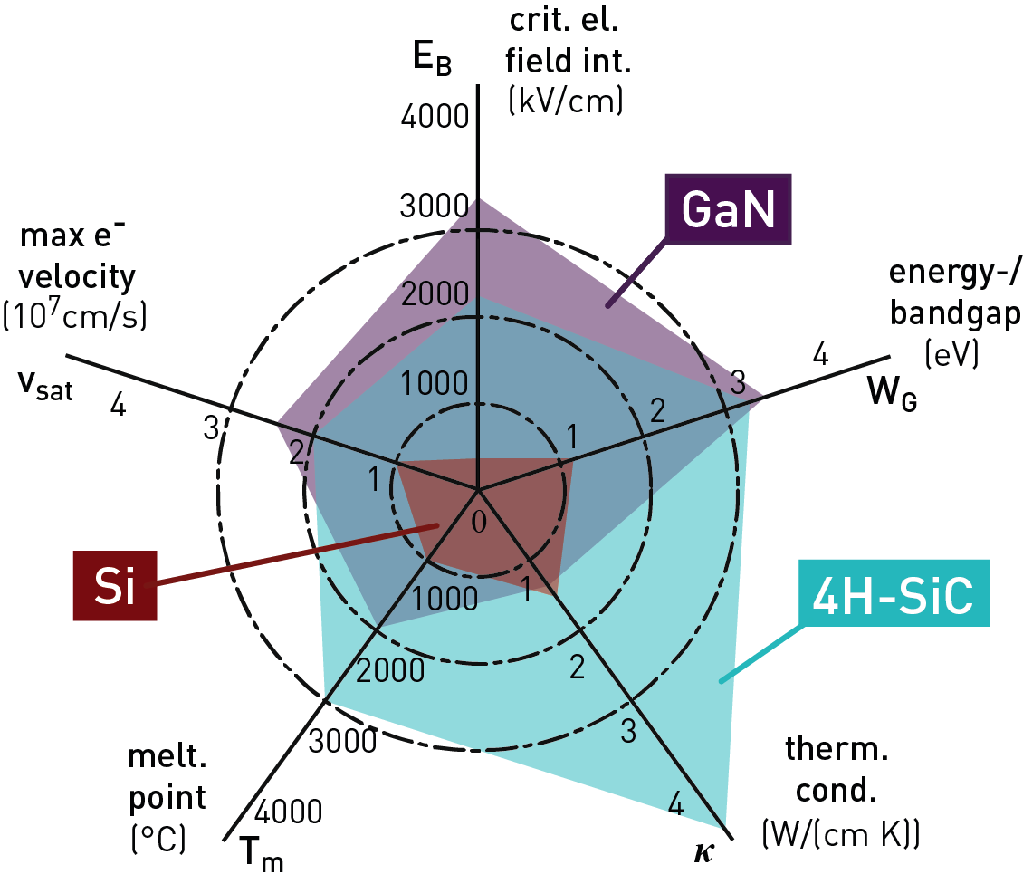
Wide bandgap materials exhibit a range of superior properties compared to conventional silicon. These components can operate at higher temperatures, offer improved blocking voltage characteristics, and enable faster switching. As a result, they can be operated with lower losses, even in the same form factor, which allows for smaller heat sinks. Higher switching frequencies generally lead to more compact filter arrangements and improved system dynamics.
Advantages of Wide-Bandgap Semiconductors
- Operation of semiconductors at higher maximum chip temperatures
- Improved power density of components
- Reduced semiconductor losses
- Increased system dynamics due to operation at higher switching frequencies
- More compact chip size with the same maximum blocking voltage rating as silicon components, or higher blocking voltage compared to similar silicon chip dimensions.
Wide-Bandgap Semiconductors: Development and Testing of Prototypes
The AIT provides a comprehensive range of services and expertise, offering scientific and applied knowledge in the field of wide-bandgap (WBG) semiconductors and delivering tailored solutions. With in-house design, development, and testing facilities, we can flexibly and efficiently address individual requirements. Additionally, we actively support the preparation of research proposals and coordinate R&D projects to ensure innovative outcomes.
AIT offers wide-bandgap semiconductor-based solutions for various applications and technical fields, including AC/DC, DC/DC, and DC/AC converters for photovoltaic systems, wind turbines, EV charging applications, drivetrain systems, data center applications, aviation, aerospace, and maritime systems.
Testing and Characterization of New Wide-Bandgap Components and Packages
In our research and development efforts, we focus intensively on testing new wide-bandgap devices and their packaging, such as top-side cooling. A core element of this process is designing and building optimized test benches specifically for wide-bandgap devices. These test benches verify system-relevant parameters such as switching and conduction losses. Additionally, we explore the hybridization of wide-bandgap devices with others based on alternative wide-bandgap materials or conventional materials like silicon to develop innovative, high-performance, and cost-efficient solutions.
Development Support for Wide-Bandgap Converters
We actively assist in the design of wide-bandgap converters through a comprehensive analysis of system layouts. Our expertise encompasses various topologies, including two-level, multi-level, and multi-cell structures, to deliver tailored solutions. This extends to single-phase and three-phase systems as well as low- and medium-power applications. To optimize system power density, increase voltage ratings, or enhance current-carrying capacity, we also offer series and/or parallel configurations. Moreover, we provide support in designing efficient cooling concepts and developing input/output filters and magnetic components for holistic solutions.
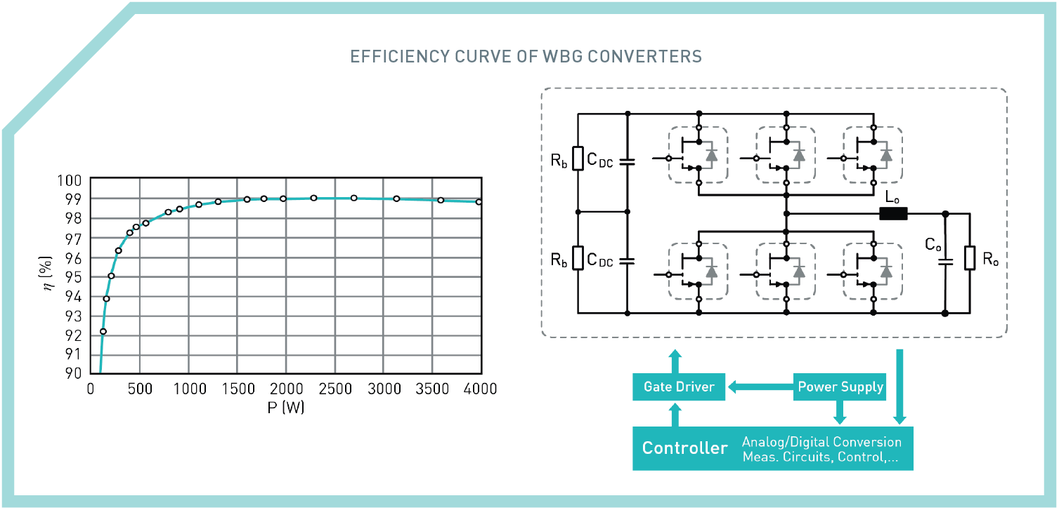
Efficiency Curve of Wide-Bandgap Converters
Wide-bandgap power semiconductors offer numerous optimization possibilities. For instance, parallel connections of devices or entire converter stages can enhance power density. Multi-cell or multi-level approaches can increase blocking voltage capability, facilitating wide-bandgap access to medium- and high-voltage applications. Additionally, resonant topologies are employed to maximize the efficiency of wide-bandgap systems. Wide-bandgap semiconductors are poised to transform the industry by enabling compact, efficient, and versatile power conversion solutions for next-generation technologies.
PROTOTYPICAL IMPLEMENTATION AND VERIFICATION
We offer comprehensive services in the area of prototypical implementation and verification. Our support includes the design and creation of schematics and PCB layouts using OrCAD or equivalent PCB design software. After development, we proceed with the initial commissioning of the demonstrator. Following this, we conduct extensive testing of the complete system to evaluate its functionality and performance. Finally, we provide a detailed report or lab test report documenting the results and insights.
